In the early days, chip designers had to rely on time-consuming simulation results or wait for the engineering sample to validate whether the design meets its intended objectives. With the increasing complexity of SoC designs, the need to accelerate software development has also risen to ensure a timely entry to market.
In the pursuit of accelerating the verification process, FPGA prototyping has become an integral SoC development tool. FPGA prototyping capitalizes on the reconfigurability of FPGA logic and its flexible IOs, enabling a cost-effective and efficient means of validating designs when compared to simulation and emulation.
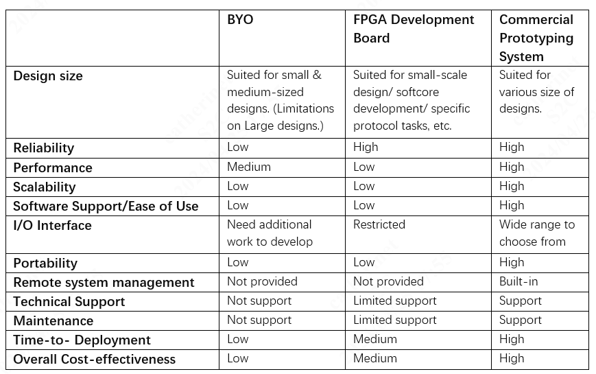
FPGA prototyping tools are generally made available from three sources: FPGA boards designed in-house by IC design companies (Build Your Own, BYO), evaluation boards sold by FPGA vendors, and commercial prototyping systems developed by EDA companies. With the rise of commercial solutions, FPGA prototyping now plays an important role of chip design and software development. This table compares the three types of FPGA prototyping.

While Build Your Own (BYO) can provide a highly customizable “made-to-order” solution, such path would require design expertise spanning FPGA system development, PCB design, and manufacturing, making the process to be manageable only if the design size is small to medium-size or a large team is dedicated to the project; time and resources to conduct iterative testing to ensure stability and reliability is also a challenge. This challenge is not an issue for FPGA development boards from FPGA vendors as the boards are made in bulk; but the capacity offered by FPGA development boards are generally are more limiting, the boards cannot be combined to scale, and IO count and the IO interface selections are often limited.
In contrast, commercial prototyping systems, such as those from Haps from Synopsys and Prodigy from S2C, excel in capacity, scalability, and ease of use. With the high stability and performance, commercial solutions provide an effective means to accelerate hardware verification and software development, also enabling early customer engagements with functional SoC prototypes and demos.
Taking S2C's solution as an example, the Prodigy FPGA prototyping offers a wide choice of models in single, dual, quad, and octa FPGA configurations and a large selection of daughter cards for fast-to-deployment. With prototyping capacities ranging from small & medium sizes to support IP verification and software development, to hyperscale designs targeting AI and 5G needing multiple systems cascaded together with partitioning support, S2C has it all covered.

In the next post, we'll dive deeper and explore the common problems encountered during functional verification and how S2C's tools can be used to overcome these challenges.
S2C is a leading global supplier of FPGA prototyping solutions for today's innovative SoC and ASIC designs, now with the second largest share of the global prototyping market. S2C has been successfully delivering rapid SoC prototyping solutions since 2003. With over 600 customers, including 6 of the world's top 15 semiconductor companies, our world-class engineering team and customer-centric sales team are experts at addressing our customer's SoC and ASIC verification needs. S2C has offices and sales representatives in the US, Europe, mainland China, Hong Kong, Korea and Japan.
 Back to list