Imagine being able to download a full-length HD movie to your mobile device in a matter of seconds, video chat with someone so remote it feels like they are sitting right across from you, or to detect and avoid sudden accidents from the sensors in your autonomous car. All of these scenarios are real possibilities in the near future if complexities in design can be overcome. This type of service ubiquity and superior user experience with faster speeds and increased capacity is what is pushing the move to 5G communication networks.
Beyond the massive bandwidth capabilities, these 5G networks will require vast meshes of interconnectivity, energy efficiency, intelligent cloud architectures, and significantly reduced latency. These essential factors are driving estimates of 5G gate sizes to be 50 to 100 times that of 4G. In addition, new WIFI standards will unveil new needs that will drive up complexity in the design even more.
With the explosive growth of IoT, the next generation of networks must provide significantly faster data speeds, ultra-low latency, and the ability to seamlessly connect billions of devices. The complexity gap between 4G and 5G networks and that of today's processors is a hurdle that must be overcome by processor vendors quickly if these vendors are to remain competitive. Engineers of these devices need efficient and effective design and verification solutions and methodologies to close the complexity gap.

While fpga emulation can certainly handle capacity requirements, designers typically need multiple replicates to perform parallel testing making emulation too expensive. The unwieldy nature of emulation systems also makes them impractical for field-testing-something often needed when developing communication systems. FPGA prototyping address this cost/efficiency issue head on as it is the only technology that can run the substantial amount of required regression tests fast enough and in the most cost effective manner. The latest FPGAs such as Xilinx's Virtex UltraScale and Altera's upcoming Stratix 10 can easily handle the large capacity that is inherent in network designs. In addition, prototyping technology advances in areas of partitioning and multi-FPGA debug have allowed FPGA-based prototyping to scale to address designs of up to 1.5 billion gates.
S2C's Prodigy FPGA Prototyping Logic Modules provide the scalable architecture that produces the best results. When combined with our Prodigy Cloud Cube™ enterprise-class system that supports up to 32 FPGAs, designers can reach their full capacity potential. Using our Prodigy Logic Modules with the latest FPGA technology allows designers to perform the requisite in-circuit testing with high-speed I/Os and Transceivers running at 1.2G LVDS and 12.5G respectively. We also offer the widest selection of daughter cards to run in-circuit testing while our design services team has the knowledge and experience to develop custom daughter cards to meet the discriminating needs of communication networks. Our prototyping systems are also one of the most compact on the market making them ideal for testing in the field.
The inherent time-to-market pressures brought on by the heavy competition in the communications sector has lead many developers to adopt FPGA prototyping. Prototyping offers a way to demonstrate a finalized product much earlier with significantly less risk than traditional ASIC design and verification. Due to the substantial increase in FPGA capacity, today's FPGA prototyping platforms can handle even the largest and most complex designs with high performance and precision. Unlike simulation that only provides an "imitative" representation, prototyping provides a real model of the design by converting algorithmic design ideas into real-time scenarios.
The ability to link the FPGA models with communication standard-compliant development tools is crucial. Transaction-level interfaces play a critical role in being able to bridge the abstraction level between behavioral models and live hardware. These transactors offer a way to communicate between software running on a host and an FPGA-based prototyping platform that often includes memories, processors, and high-speed interfaces.
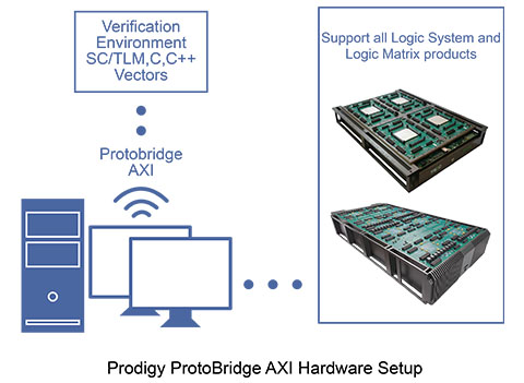
S2C's unique patent-pending Prodigy ProtoBridge™ System is a solution that allows for just this type of high-speed communication. ProtoBridge supplies a transactor interface between a software program and the world of AXI-compliant hardware. There are two key parts to this: an AXI-to-PCIe bridge that connects to a host computer, and a C-API that communicates to the design through the bridge. The software-to-AXI transactor offers new flexibility to designers building ARM-based systems. And coupling this to a PCIe interface supporting transfer speeds up to 1000 Mbytes/sec, provides a perfect development platform for data-intensive applications.

A system like this allows designers to maximize the benefits of fpga based prototyping much earlier in the design project for algorithm validation, IP design, simulation acceleration and corner case testing. A prototype combined with a transactor interface makes a range of interesting applications possible throughout the design flow.
S2C's entire Prodigy Complete Prototyping Platform provides solutions for every aspect of your design and can be seamlessly incorporated into the original ASIC design flow. We provide the most comprehensive array of prototyping logic modules to fit your design size as well as the largest library of pre-tested prototyping IP and reference design flows to speed up and simplify your prototyping process. Our Prodigy Cloud Cube that when combined with our Neuro software to manage parallel/remote software development can be used as a regression farm for automotive applications. The patent-pending Prodigy ProtoBridge System allows for high-speed communication between software running on a host and an FPGA-based prototyping platform through the use of transactors. Our Prodigy Player Pro Software helps to configure the prototype and provides remote system monitoring and control. The compile functionality within Player Pro offers advanced partitioning and the soon to be released Prodigy Multi-Debug System will relieve the arduous and error-prone task of debugging each FPGA manually. S2C's suite of Prodigy FPGA-based prototyping solutions is the most comprehensive on the market to help you realize the genius of your next design.