by Don Dingee on 08-30-2022 at 6:00 am
Categories: EDA, Prototyping, S2C EDA
When discussing FPGA-based prototyping, we often focus on how to pour IP from a formative SoC design into one or more FPGAs so it can be explored and verified before heading off to a foundry where design mistakes get expensive. There's also the software development use case, jumpstarting coding for the SoC before silicon arrives. But there is another shift left use case – closer to project start when a pile of IP in the prototyping platform is tethered to a development host looking for signs of life. Creating a fast, productive prototyping device-under-test connection is the topic of a new white paper from S2C.
Facing the classic embedded design bring-up conundrum
Embedded designers have faced a similar board-level challenge for years. Bringing up a board requires being able to see into it with some interface. But a complex interface like USB requires both working hardware and a protocol stack for communication. When it works, it's great. When it doesn't, it can be hard to get visibility into what's wrong. Ditto for other complex blocks where visibility is challenging.
Running around the board's interior with a logic analyzer gets is where the fun, or lack thereof, begins. Traces may be tough to probe. Getting stimulus and triggering right to see the problem as its happening can be elusive. Moving a wide bus setup to different points around the board takes time. The more logic gets swept up into large devices like ASICs and FPGAs, the harder physical probing gets, and the more visibility drops.
Hoping to solve visibility in the embedded world, JTAG emerged first as a simple daisy-chain connection between chips or logic blocks inside an ASIC or FPGA. A JTAG analyzer is a simple gadget with four required wires and a fifth optional wire. The scheme works, but it can be painfully slow. If one is to solve the bring-up conundrum on an FPGA-based prototyping platform, which is a complex board with some big FPGAs, something much better is needed.
Moving to native interfaces on both sides of the workflow
Fortunately, two interfaces exist that fit perfectly into an FPGA-based prototyping device-under-test connection.
-AXI is a ubiquitous native interconnect between IP blocks on the device-under-test side. It's a single initiator, single target protocol in basic form, but it extends easily into an N:M interconnect that can scale topology for connecting more IP blocks.
-PCIe is easy to find in or add to development hosts. It's fast, cabling is simple, and a host device driver is straightforward.
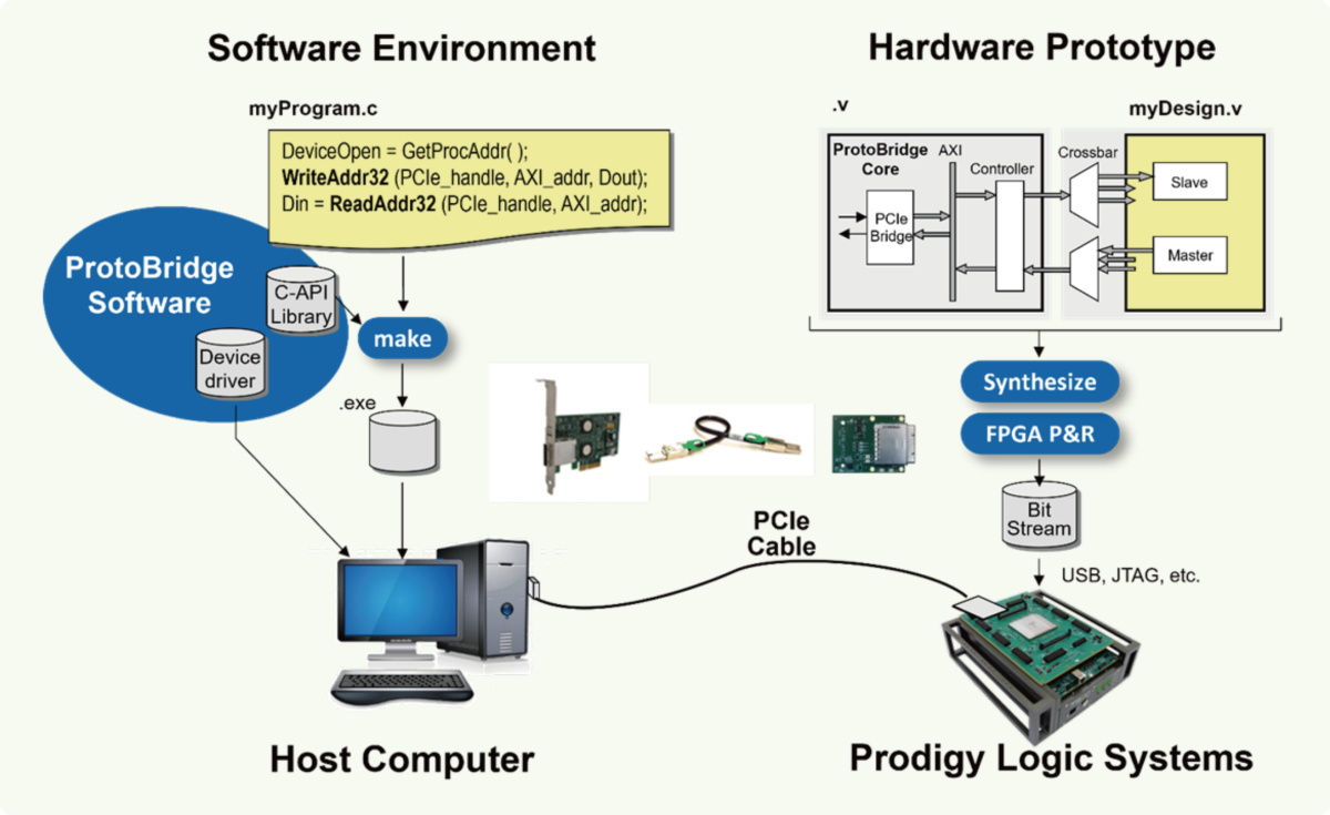
S2C brings in the ProtoBridge System, a transactor-level interface with speed and visibility that improves test coverage and productivity, especially in the early phases of design. Here's a conceptual diagram.

Transactors offer a way to bridge the gap between behavioral models typical of a test and verification environment and RTL models running in hardware on the FPGAs. The other benefit is that it allows software developers and test engineers to work in a familiar environment, C/C++, instead of RTL or FPGA constructs.
And the requisite speed is there. Some tests may require transferring big stimulus files, like videos or complex waveforms. Stimulus can be stored on the host until needed for a test, then transferred for execution at full PCIe bandwidths up to 4 Gb/sec.
As the project progresses, things shift from an initial bring-up mode to test coverage mode. The ProtoBridge scheme remains the same from start to finish, so teams don't have to bring an array of different tools to the party. Workflows are smoother, productivity improves, and time is freed up for deeper exploration and testing of designs – all benefits of a shift left strategy.
To get the entire white paper and see the rest of the S2C story on the high bandwidth prototyping device-under-test connection and more background on ProtoBridge, hit the link below, then scroll down to this title:
White paper: High-bandwidth PC-to-DUT Connectivity with ProtoBridge