Innobase started its business in 2021 to develop SoCs for mobile communications with a focus on technologies for IoT applications. Adapted to 4G/5G networks where low cost, low latency, and massive connectivity are key industry imperatives, Innobase specifically targets the Consumer, Industrial, and Municipal markets, including,
- Consumer – wearable devices, bicycle sharing, and smart home
- Industrial – UAVs (Unmanned Aerial Vehicles), logistics tracking, and industrial control
- Municipal – monitoring systems, intelligent traffic, and the Smart City
During the development of complex SoCs, popular verification wisdom is to apply as much real-world stimulus to the SoC design as possible during design verification to confirm that a design will operate as expected in the end-product – prior to committing the design to silicon. In the case of 5G chipsets, the real-world stimulus includes testing complex communication protocols, data encoding techniques, modulation methods, and running hardware-dependent software on the design prototype – all with the added verification complexity of a variety of different 5G chipset operating modes. This is a monumental verification challenge and can only be accomplished by running the SoC design at hardware speeds connected to real system hardware.
Innobase implemented a comprehensive SoC verification flow for its 5G chip platform, including S2C's FPGA prototyping hardware, a powerful segmentation engine to improve performance and efficiency, S2C's prototyping software and deep-trace debug tools, and S2C's Prototype-Ready IP – for pre-silicon verification of its 5G physical-layer designs. While other tools were part of Innobase's verification flow for surgical verification of short periods of chip operation, only prototyping could enable Innobase to achieve sufficient operational testing of their 5G SoCs prior to silicon.
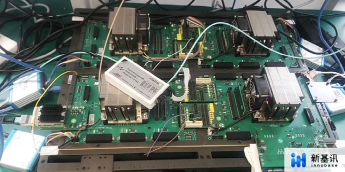
Innobase's fpga based prototyping platform was connected directly to bench-top instrumentation during SoC development to apply 5G communications traffic to the FPGA prototype at hardware speeds and confirm the correct operation of the communication system uplink, and board-level system operation of the 5G physical-layer functionality. With the addition of FPGA prototyping, Innobase was able to “shift-left” their chip development process to include early hardware/software co-development.
Innobase chose S2C's Prodigy S7-19PQ Logic System for prototyping its 5G chips. The S7-19PQ Logic System includes four (4) large Xilinx FPGAs (Virtex UltraScale+ VU19P) in a single integrated chassis with board-level connectors designed for reliable FPGA-to-FPGA interconnect, and to plug-and-play with the real-world through cables and daughter cards (S2C's “Prototype-Ready IP” or customer-designed daughter cards).

S2C offers a broad selection of prototyping hardware platforms based on popular Xilinx and Intel prototyping FPGAs for different prototyping requirements, and prototyping accessories designed and built to operate seamlessly with S2C's prototyping hardware platforms for complete prototyping solutions.
Innobase is a professional wireless communication chip manufacturer with 5G/4G technology as its core. Innobase focuses on mobile communication technology for IoT and baseband SoC chip products. Our team consists of seasoned chip designers and communication engineers, many of whom worked at leading smartphone chip suppliers. Key team members have 20+ years of experience in modem technology. The Innobase team includes over 100 R&D staff members at four locations in China: Shanghai, Nanjing, Chengdu, and Zhuhai.
S2C is a leading global supplier of FPGA prototyping solutions for today's innovative SoC and ASIC designs, now with the second largest share of the global prototyping market. S2C has been successfully delivering rapid SoC prototyping solutions since 2003. With over 500 customers, including 6 of the world's top 15 semiconductor companies, our world-class engineering team and customer-centric sales team are experts at addressing our customer's SoC and ASIC verification needs. S2C has offices and sales representatives in the US, Europe, mainland China, Hong Kong, Korea, Japan, and Taiwan. For more information about S2C’s FPGA-based prototyping solutions, and how to contact us, please visit our website at s2cinc.com.