S2C's FPGA Prototyping Solutions
by Kalar Rajendiran on 02-10-2022 at 10:00 am
Categories: EDA;Prototyping, S2C EDA
Prototyping solutions have been in the news a lot lately. And FPGA-based prototyping approach is pretty widely used. On a panel session at DAC 2021, Amir Salek, Head of Silicon for Cloud and Infrastructure at Google had the following to say. Prototyping FPGA is a tremendous platform for testing and validation. We are doubling down on emulation and prototyping every year to make sure that we close the gap between the hardware and software.
With unrelenting time to market pressures, companies deploy different tactics to compress their product development cycles. As a product launch requires having both the hardware and software ready at the same time, companies seek a head start on software development. Rather than waiting for their chips to be ready in final form, they leverage FPGA prototyping to develop and test their software. And hardware/software co-verification is an important aspect of product development, for integration of software with hardware well before final chips and boards become available.
While FPGA with its flexibility lends itself nicely for implementing prototypes of very complex, high-performance SoCs, they do come with some drawbacks. One of those drawbacks being that they trail in terms of supporting the most advanced connectivity interface speeds. System interfaces such as PCIe, DDR, HBM, etc., have been evolving rapidly to support faster and faster data transfer speeds. While mainstream FPGAs can fit large SoCs, they lag when it comes to supporting the most advanced interface speeds. More advanced FPGAs can support the latest PCIe speeds, but they cannot yet fit large SoCs.
S2C solved the above dilemma through a partnered solution with Avery Design Systems. Avery's PCIe and memory speed adapters can be synthesized into S2C's FPGA prototyping platforms to support up to PCIe 6.0, HBM3 and LPDDR5 protocol interfaces. You can learn more about this S2C-Avery partnered solution from a recent SemiWiki post. That post provided just an overview of S2C's product offerings, as its primary focus was on Avery's speed adapters. The speed adapters cannot do their part without a complete FPGA prototyping platform.
As a global leader of FPGA prototyping solutions, S2C has been delivering rapid prototyping solutions since 2003. S2C offers many different product lines leveraging both Intel and Xilinx FPGAs. Their solutions can fit a wide range of design sizes and support advanced interface speeds as well. Here is a short video clip about their Prodigy Logic Matrix LX2 prototyping solution. The following is a summary of their range of platforms and accompanying productivity tools.
S2C's offerings cover the prototyping needs of the spectrum of high-end, mainstream and cost-sensitive market driven designs.
The Prodigy Logic Matrix is built to address the highly complex, high-performance, large SoCs used in applications such data center, AI/ML, 5G and autonomous driving. It is a high-density FPGA prototyping platform that is optimized for space and connectivity. It is designed for multi-system expansion to support billions of ASIC gate capacity.
The Prodigy Logic System series is a compact, sleek, all-in-one design that offers maximum flexibility, durability and portability. Both Xilinx-FPGA-based and Intel-FPGA-based versions of these systems are available to match customers' preferences.
The Prodigy Logic Module series is specially designed with low profile and affordability in mind. The Prodigy Logic Modules are based on Xilinx's KU and K7 FPGA devices.
S2C's Productivity Tools
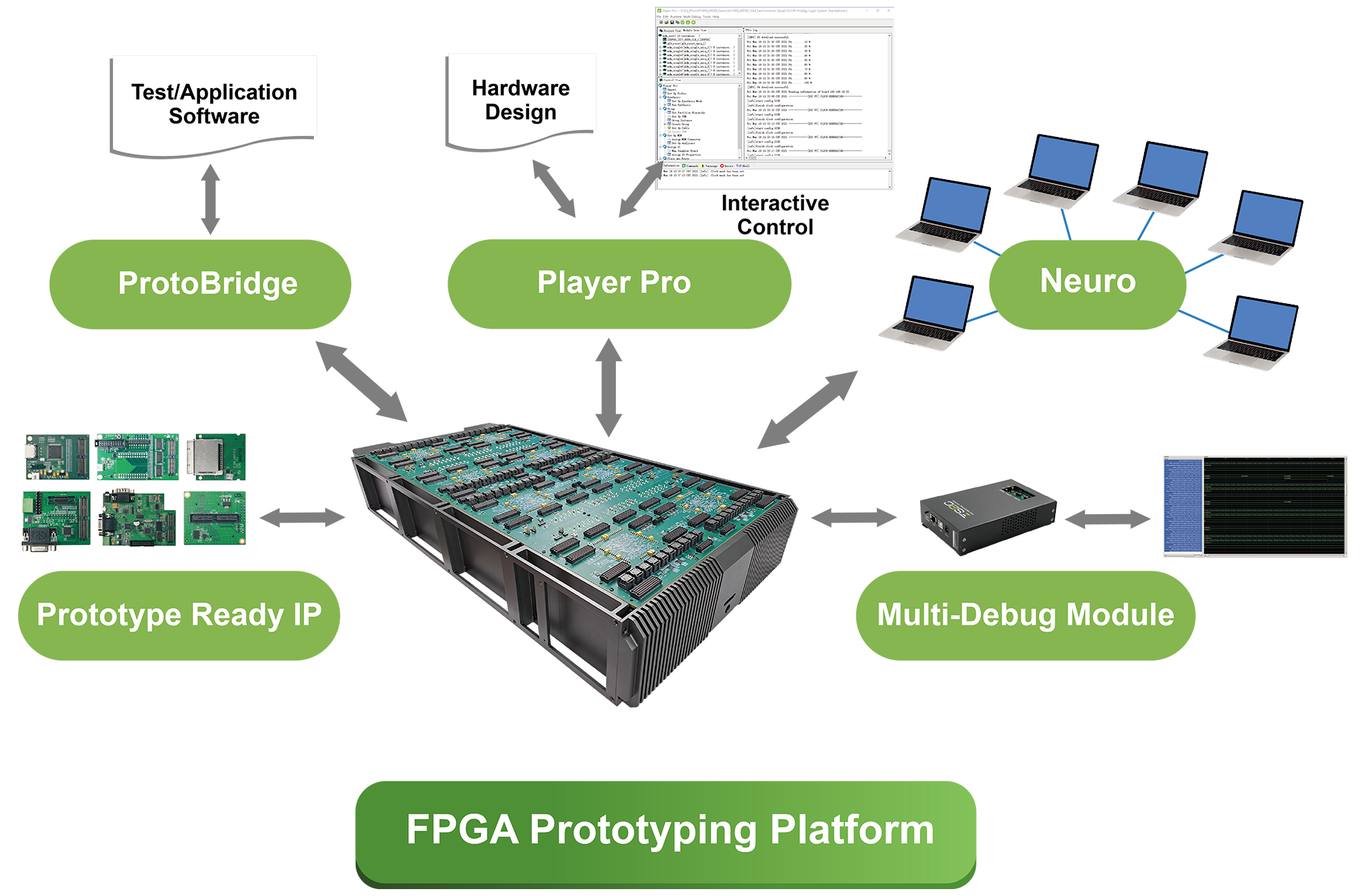
S2C's prototyping solutions are accompanied by a suite of productivity tools that eases the setup, development, test and validation process.

PlayerPro
Prodigy PlayerPro is a tool that offers an integrated GUI environment and Tcl interface and works with their prototyping platforms. It makes it easy to take an existing design, compile it, partition into multi-FPGAs, and generate the individual bit files. It also runs remote system management and provides setup for multi-FPGA debugging.
ProtoBridge
Traditionally, realizing the full benefits of a prototyping platform meant investing in additional hardware and other resources. With ProtoBridge, customers can leverage as much of their existing resources. For example, they can use a PC's memory to store data rather than providing additional memory on the design under test. Use the prototyping platform with other commercial or in-house verification tools through C-based API over standard AXI. IP blocks connected to the AXI bus can be verified without processor cores or peripheral blocks. For all the details, refer to Prodigy ProtoBridge page.
Neuro
Neuro enables multi-dimensional management of resources over multiple projects and users. It helps optimize resource utilization by enabling users to quickly access FPGA compute power and CPU clusters wherever they may reside. This allows S2C's customers to leverage their in-house resources as well as cloud-based resources.
Prototype Ready IP
S2C provides a large library of off-the-shelf interfaces and accessories for FPGA-prototyping. All interfaces and accessories work with the Prodigy Logic Modules to further speed up and simplify the system prototyping process. Accessory modules are supplied as daughter boards that plug into the Prodigy Logic Module, providing pre-tested interfaces and reference design flows for easy bring-up.
S2C also provides professional services to customize interface and accessory modules to meet their customers' application needs.
Multi-Debug Module
The S2C Prodigy Multi-Debug Module is an innovative debug solution for FPGA prototyping. It has the ability to run deep-trace debugging simultaneously on multiple FPGAs. It can trace up-to 32K signals per FPGA in eight groups of 4K signals each without re-compiling. It can store 8GB of waveform data without consuming user memories.
Availability
S2C FPGA prototyping products are in stock now and customers can get their hands on them with a short lead time. While the industry is facing supply chain constraints, this is refreshing to hear. For more information, contact S2C.