Prototype-Ready IP jump starts complex SoC Integration with 3D Graphics
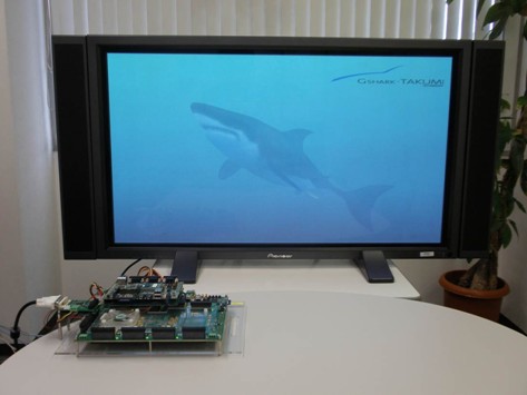
San Jose, CA – July 2, 2012- S2C announces that TAKUMI Corporation, a Japan-based advanced Graphics Intellectual Properties (IP) provider, has implemented a series of Graphics IP cores on S2C’s rapid FPGA-based prototyping systems including GS3000 and GSV3000 cores. These TAKUMI IP cores have been fully validated in FPGAs and can be easily demonstrated to and evaluated by customers; thereby significantly reduce system-on-chip (SoC) integration time.

TAKUMI&rsquo's GSHARK family of IP is the graphics solution to accelerate display rendering on a variety of embedded systems including mobile devices, digital home appliances and in-car information systems. Uniquely designed and customized to support embedded systems, GSHARK-TAKUMI family extensively lines up graphics IP cores addressing different embedded system use models, for the best IP selection.
Toshio Nakama, S2C&rsquo's Chief Executive Officer, said,” Integrating a complex IP core, such as a 3D graphics IP, in an SoC design often requires a tremendous amount of verification effort such as verifying the correctness of all hardware functions, evaluating SoC bus efficiency and testing software compatibilities. And, the best methodology today for performing these tasks is by using FPGA-based prototypes that closely resemble the entire design operating at or close to actual speed, many months before actual silicon is available. We are very pleased to work with TAKUMI to provide SoC developers a series of advanced graphics IP cores already mapped on FPGA-based prototypes that can significantly shorten IP integration into SoC design and allow early start of software development and testing.”
“ Graphics IPs today are very complex and require a large number of test patterns to perform the complete hardware verification and software testing. Thus, a reliable, flexible and high-performance FPGA platform is required,” said Hiroyuki Nitta, Executive Director of Research and Development of TAKUMI Corporation. “We have selected S2C as our preferred FPGA platform partner because their products are known for their reliability, interface flexibility to a variety of SoC models and interfaces, and scalablity to support designs of various gate counts.”
TAKUMI&rsquo's Graphics IP cores were prototyped and available as reference designs today on S2C&rsquo's Virtex-6 760 TAI Logic Modules. The reference designs can be easily ported to the new Virtex-7 2000T TAI Logic Module series or the Altera Stratix-4 820 TAI Logic Module series upon request. S2C&rsquo's complete suite of Rapid FPGA-based Prototyping solution is designed to make prototyping a pleasant experience for designs of any size from 2 million to up to 180 million ASIC gates with 1 to 9 FPGA devices on a single board. In addition, S2C provides a complete solution with prototype creation and debug software; DPI, SCE-MI and C-API co-modeling; and, a large library of Prototype Ready IP & Accessories.
About TAKUMI
Founded in 2003, TAKUMI licenses out its unique and OpenGL ES- and OpenVG-compliant Graphics Accelerator IP cores for embedded systems and mobile information devices, including digital still/video cameras, mobile phones and set-top boxes that enable the smallest size and power consumption as well as real rich 2D/3D intuitive user interface around the world. The company maintains headquarters in Shiba, Tokyo. TAKUMI also has offices in Kofu, Yamanashi.
About S2C
Founded and headquartered in San Jose, California, S2C has been successfully delivering rapid SoC prototyping solutions since 2003. S2C provides:
Rapid SoC FPGA-based prototyping hardware and automation software
Prototype Ready™ IP, Platforms, and Accessories
System-level design verification and acceleration
S2C's value is our singular focus on SoC/ASIC development. Our highly qualified engineering team and customer-focused sales force understands our customers’ SoC development needs. S2C&rsquo's unique FPGA-based solution, using our patented TAI IP technology, enables designers to quickly assemble FPGA-based SoC prototypes on S2C FPGA boards. This gives customers an early start on software development, typically the long pole item in development schedule. Combining rapid prototyping methodology with a comprehensive portfolio of Prototype Ready IP and advanced verification and acceleration solutions, S2C solutions greatly reduce the SoC design cycle.
In addition to the headquarters in San Jose, CA, S2C currently has 4 direct offices located in Shanghai, Beijing, Shenzhen China and HsinChu, Taiwan. S2C is also the organizer of the annual SoCIP seminar and exhibition in China, which brings SoC designers from the Asia-Pacific region together with international silicon IP and SoC solution vendors.