by Daniel Nenni on 12-05-2023 at 10:00 am
Categories: Chiplet, EDA, FPGA, Prototyping, S2C EDA
S2C has been successfully delivering rapid SoC prototyping solutions since 2003 with over 600 customers, including 6 of the world's top 10 semiconductor companies. I personally have been involved with the prototyping market for a good part of my career and know S2C intimately.
S2C is the leading independent global supplier of FPGA prototyping solutions for today's innovative SoC and ASIC designs, now with the second largest share of the global prototyping market. We all know the benefits of working with an independent company that can focus on the specific needs of prototyping customers so I will skip forward to the technology part of this article.
For prototyping we all read about the scalability of the systems and how many gates are supported. Today hyperscale designs that are in the billions of gates can be prototyped using the latest FPGAs from Xilinx. These high-end prototyping systems are generally housed in a dedicated facility or a cloud.
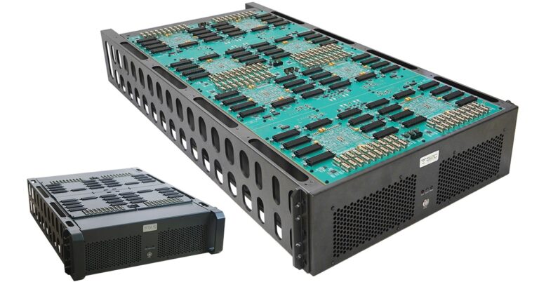
Not all designs are in the billions of gates however and now that we are entering the chiplet era smaller designs are a focus and that brings us to the new S2C Prodigy Logic Matrix LX2 Mini, an enterprise-class FPGA prototyping solution designed for lab or desktop use.


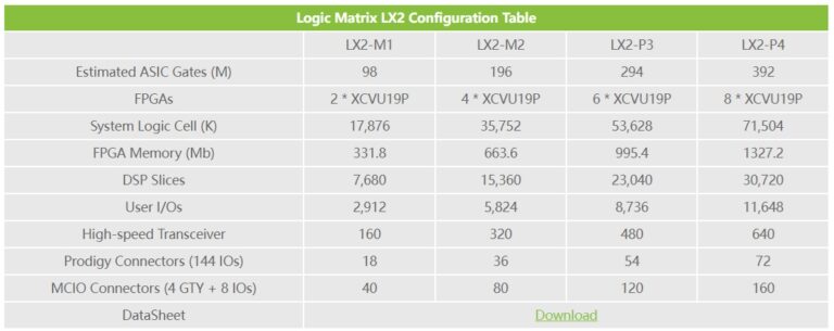
Despite its smaller form factor relative to LX2, LX2 Mini also delivers the same high bandwidth and scalability. Both LX2 and LX2 Mini can leverage S2C Chiplink AXI IP, enhancing partition interconnectivity at up to 100MHz.
Here is a quick video on the S2C Prodigy Logic Matrix LX2 Mini:
Brining the full power of S2C Prodigy Logic Matrix Prototyping to the desktop with the mini series of enterprise-class prototyping will further enable the chiplet market.
Chiplets are like the building blocks of a computer chip. Instead of creating a single, monolithic integrated circuit, chiplets are smaller, individual semiconductor components that can be designed and manufactured separately. These chiplets can then be combined or stacked together to form a more complex and powerful integrated circuit.
The idea is to take advantage of specialized manufacturing processes for different components of a chip. For example, one chiplet might be optimized for high-performance computing, while another might be designed for energy efficiency. By combining these chiplets, you can create a more flexible and efficient overall system.
Think of it like assembling a puzzle where each piece is a specialized chiplet, and when they come together, they create a powerful and cohesive unit.
Verification is a crucial step in the design and manufacturing process of chips, especially in the context of chiplets. Since chiplets are separate components that come together to form a single integrated circuit, verifying their functionality individually and as a collective unit is essential.
Clearly FPGA prototyping chiplets will dramatically speed the verification process and if you are delivering a chiplet to a customer the new S2C Prodigy Logic Matrix LX2 Mini can be sent to your customer’s desktop for close collaboration, absolutely.